The process in which I used to make PCBs at home has changed a lot in these recent months.
Now I use Eagle CAD program to draw the board designs. The free version of Eagle allows to design 2 layer boards within 80mmx100mm size for non-commercial use. You can download Eagle software from http://www.cadsoftusa.com/downloads/
Later someday I'll show how to extract a nice printable layout from Eagle PCB design for both copper layers and for legends.
I've found that Canon LBP2900B printer gives best ink concentration required for PCBs when compared to other printers like HP P1007 which I've used before.
Now I use glass epoxy copper laminates. I've used both phenolic paper laminates as well as glass epoxy ones and have found that the glass epoxy ones are better.
The G.E ones are surely priced double than the P.P laminates, but the G.E ones are durable and tough enough to bear much heat applied to the PCB during toner transfer or solder leveling or any other rough handling.
The POP ones bend and become very soft that they can be bend forever or break if those are exposed to the heat I use. The strength comes to GE ones from the fact that they are made of glass fibre cloth's thin layers adhered one layer with another by some kind of epoxy resin.The same technique is used to make the tough and lightweight enclosures for aeroplanes above which a thin sheet of aluminum is layered.
Oh and all responsibilities for uneven exposure in photos to my camera's flash. 😛
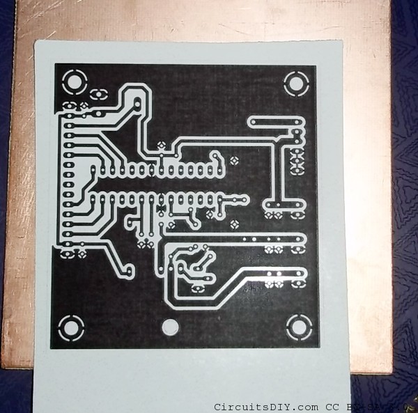
Below you can see I'm using a 10cm x 10cm copper clad board and a somewhat smaller size PCB design. The PCB pattern is printed upside down with a laser printer to a common photopaper. I've found that regular glossy photopapers makes better transfer than any other papers like magazine paper, etc. In my locality 20pcs of such papers cost only ![]() 80.
80.
For transferring the toner to the pre-sanded copper laminate, a laminator as well as a household Iron can be used. In case you are using laminator, preheat it to 200°C and once pass the blank copper laminate through it and in second time, pass the copper laminate(careful, it'll be hot) with the PCB layout facing down to the copper side. Then third pass the set again by rotating it 90° angle, that is you pass it this time left to right instead of up to down.
If you are using a iron, make it preheat to 80% maximum heat setting (cotton). Then when the iron is heated, press it to the copper laminate to heat it up and after 5-6 seconds, remove the Iron and put the PCB layout facing down towards the hot copper. Then again press the paper with the Iron at same heat settings. Be sure to heat it evenly in all sides and corners by dragging the iron in the plane. Do this until you see the white paper started turning into little brown. Stop by then. As my experience it takes 30-90 seconds depending on the board size.
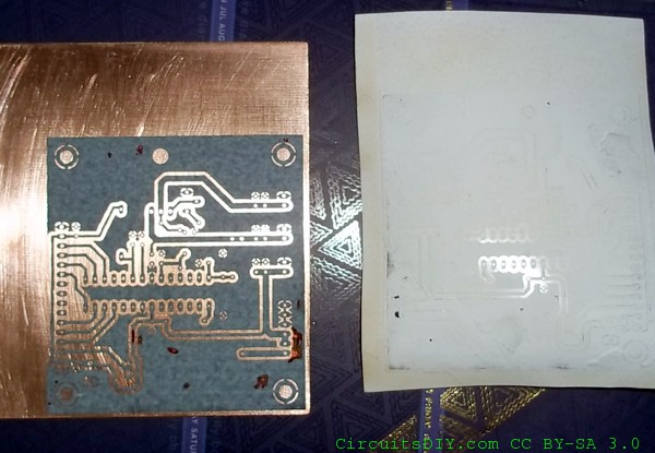
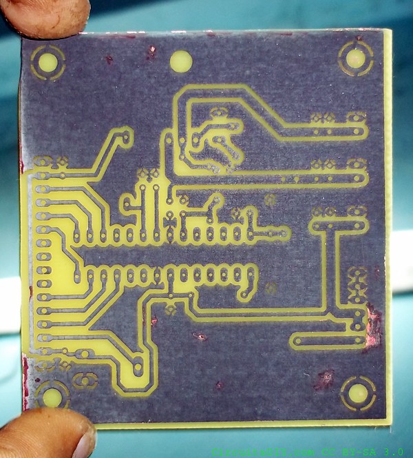
No matter which heat source you've used, you need to cool he PCB slowly by putting it inside a book and press ing the book hardly. This will ensure there is no air gap between melted toner and PCB that might cause some toner to stick to the paper and not the copper.After 2 minutes, take the PCB out and gently peel the paper from the PCB. Don't soak it in water as you might knew. No soaking in water is needed for these papers. Also soaking and peeling by fingers will require much time, but you can peel the paper off the PCB in few seconds and what you'll get is shown below. If there is any breakage in toner, you'll see small traces of black ink into the paper (See below), just fix those areas with any permanent CD/OHP marker.
In this step I cut the PCB to the desired size. You may think why I haven't cut this previously but there's no difference you can cut anytime you wish.
After cutting a good visual inspection is necessary to find any broken tracks, etc and it's the last time you fix them by marker pen.
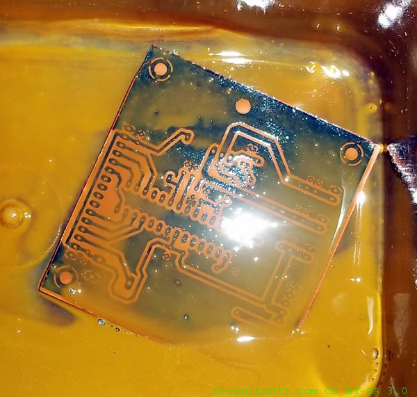
Then I dip the PCB to a plastic container partially full with ferric chloride. I don't throw used chemicals but store it by closing the lid of the container and always use used etchant and add fresh etchant to it whenever it becomes very weak.
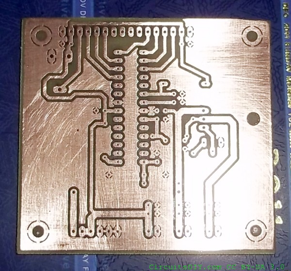
After etching completes in around half an hour, it's time to clean the PCB in tapwater. Use much water to completely remove any residuals of the etchant. True inspection of the board can be done by seeing it through light.
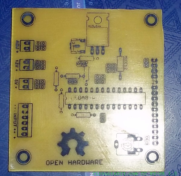
Now it's time to transfer the legend to the top of the PCB. Here the same steps are performed as it previously done while transferring the toner for PCB tracks.
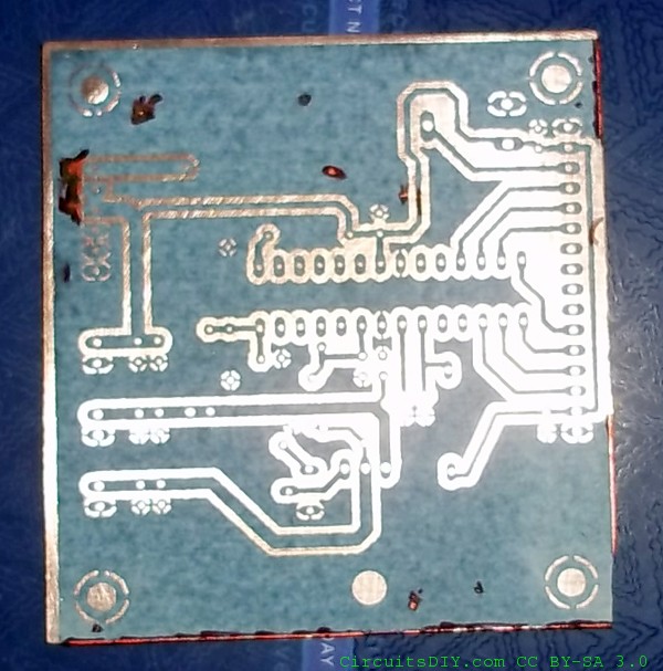
After cleaning the toner from the bottom of the PCB, the PCB looks real shiny like gems.
Next, I drill the holes using my hand drill. Unfortunately the small holes needed 0.8mm drillbits but I had 1.2mm in stock so the drilling obviously isn't looking good, but it will work anyways.
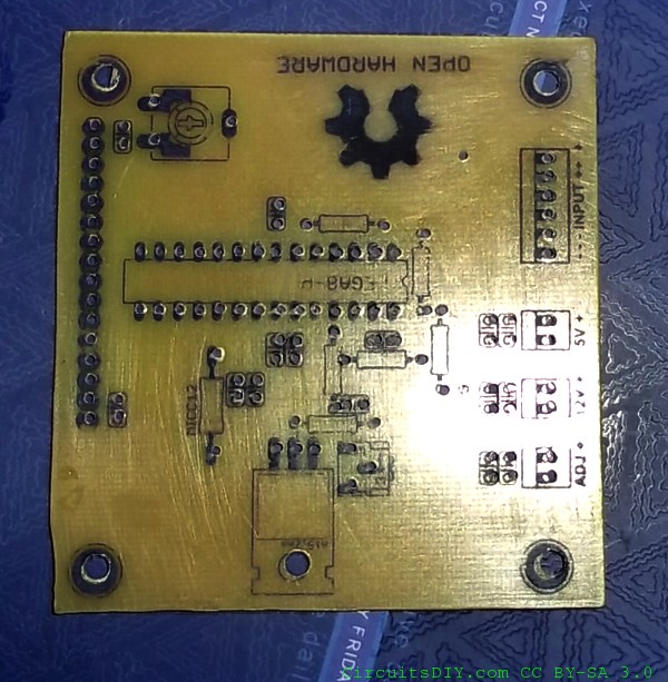
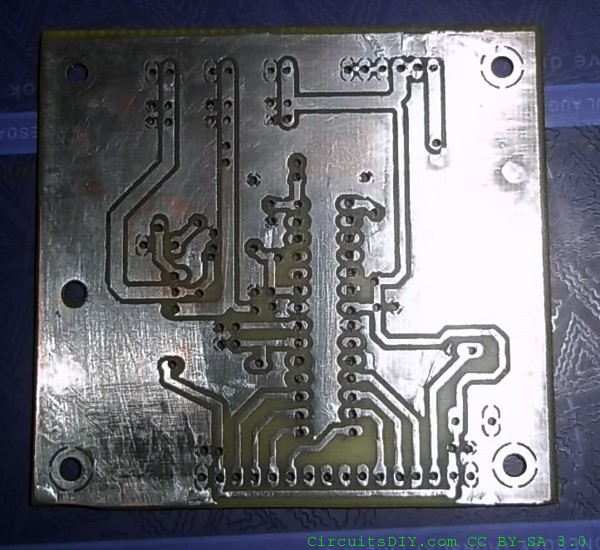
Next step is tinning/soldering the track of the PCB to prevent the copper from oxygen/water from environment. Since this particular design had copper plane, it's nearly impossible to neatly solder the pcb with soldering iron. For tinning, you need to solder here and there randomly with soldering iron. Then add lots of flux to the coppers and cover the PCB bothside with paper and pass it through 250°C heated laminator 4 times from each side totaling 16 passes. If you are using iron, heat it at maximum level and drag the iron over top paper and just drag it for 2-3 minutes. A lots of smoke will come from this step as all the flux will be used an the top paper will become brown burnt color.
Skip this step if you've used paper phenolic laminate because they cant bear this much heat and will be puffed into layers.
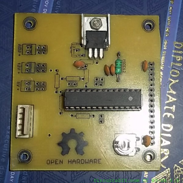
When this completes, remove paper from bothsides (the bottom paper was used to protect the legend from any scratches) and clean the PCB with a old toothbrush and Kerosene and you'll end up with a nice looking PCB like the one below.
Now it's time to put components and soldering them to get the project donw for which the PCB is made.
About the project: This in one of my upcoming projects and this will be published in this site in few weeks.
i am the very beigner of the electronics field your narration and the pictures are well understandable i really thank for your works done on this fields
Very wonderful
very simple & nice
Excellent Study material. I have a doubt. When you apply flux and cover it with paper, wouldn't it get obsorbed by the paper?
Paper can't absorb that much flux. And when it is passed through hot laminator, flux melts and does the job.
hello arup,
nice tutorial.I have been using this method for quite some time.I used to soak the board in water and peel off the paper.After the removal of the paper,sometimes the toner which didn't adhere to the copper properly got washed away and i had to depend upon marker pens and correct the missing traces.But recently I heard about making PCBs by the method of screen printing.Even if its suitable for production of boards in large quantity,can you please tell me how to do it and what are the materials required etc.
kishna
I have tried and spent more than Rs. 2000 in screen printing materials and inks for PCB making, but all wasted. Screen printing requires special skills and I was able to do it, but truely speaking, the quality of PCB layout is nice but not worth spending that much when it can be done with cheaper special PCB transfer paper.
I've been laying out PCBs since we had rolls of black tape we stuck to Mylar grids, which is a long time. We even had preprinted stickers for ICs and connectors.
Presently I have 5 software packages on my CAD designated PC and my most used layout package in the free ExpressPCB ans ExpressSCH(ematic) from http://www.expresspcb.com.
I have Eagle (Pro) version but hands down Express is better as there is no learning curve and you don't get reminders when you break the rules - which I do deliberately and often.
Express can do netlists. I occasionally import an Express schematic into Eagle just to see how it thinks the autoroute is optimum.
No software package can do the whole job, not even CIRCUIT CREATOR Platinum of which a copy sits on my workstation.
for etching a 2:1 mixture of h202 (hydrogen peroxide) and hcl can be used ....both are more easily availiable h202 is availiable in medical shops (ask for peroxide) ... and hcl is availible in general stores (the bathroom tile cleaning acid) ...this mixture is far better ... the hcl and h202 are not as corrosive as fecl3 ... and not only it etches faster
(ive done my etchings within 2 to three minutes) the only thing is that the solution should be freshly prepared and used ... the reaction is even faster becasue mixing these two makes the solution warmer ....go ahead try it out
Yep. I've heard about that too but didn't had chance to try it out.
HELLO ARUP
WHAT'S THE GREEN COLOUR COATING THAT'S APPLIED ON THE BACKSIDE OF PCBS?
It's soldermask layer. This prevents solder to flow to PCB tracks outside the soldering circle.
be careful while using this method. this process evolves hydrogen gas which has already corroded my all office equipments (metal surfaces, drill bits etc in few days). so keep the used liquid in a closed container immediately & always. but frequently open its lid as, immense pressure is developed in the closed container which may explode if neglected. the process is still very fast.
Hei
i am ajx from nepal.
I tried alot of this method. I want to know how to make pcb by screen print method? If you know this method plz reply me as a brief.
I had tried the screen print method and let me tell you the truth that the method is much more accurate but has much cost unless you are making same PCB for 100s of quantities.
plz help me here.i want raw pcb clads. i am from andhra pradesh.where can i get this.can any one sent to me in corrier.i'll pay.its urgent plz .
hi.well done.but can u give details from where we can get raw pcb clads in south india.i am from andhra pradesh.thank u,give reply.
Search in SP road, bangalore.
i am std of 10th
i want to boost 2-3 volt to 4.3 - 5 v.
because i want to charge a mobile phone.
-Saurabh (Dhule,Maharashtra)
Use AAsaver.
http://rayshobby.net/blog/?page_id=1452
The link given by you returns an error. There is no such page.
I am sorry, I forgot to look at the date of this post...lol. I guess the web page was removed long back 🙂